学习笔记-2022.1.12
1. SOC课程ppt第1-3章
Lecture 1 – Introduction
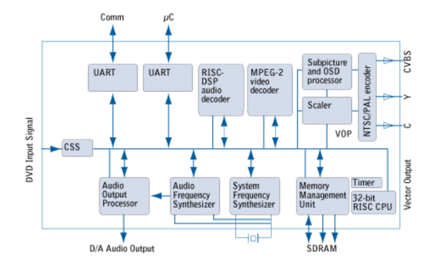
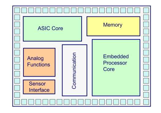
- System-on-Chip
Integrating all or most of the components of a hybrid
system on a single substrate (silicon or MCM), rather
than building a conventional printed circuit board.
(1)More compact system realization
(2)Higher speed / performance
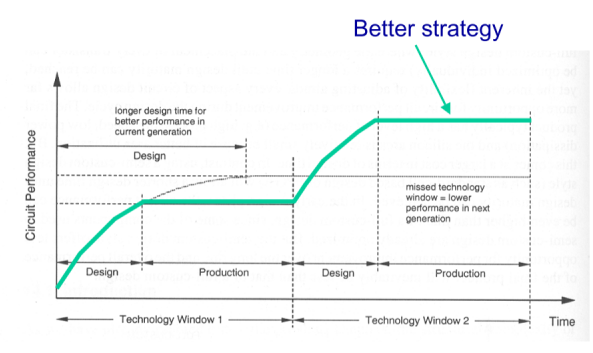
- Better reliability
- Less expensive !
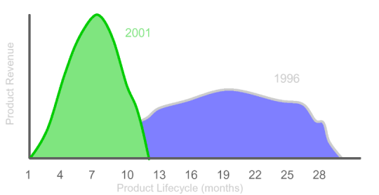
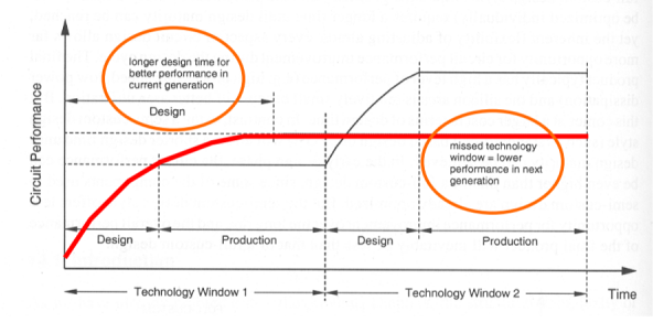
- Products have a shorter life-cycle !
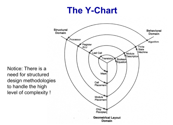
- Structured Design Principles
Hierarchy: “Divide and conquer” technique involves dividing a module into sub-modules and then repeating this operation on the sub-modules until the complexity of the smaller parts becomes manageable.
Regularity: The hierarchical decomposition of a large system should result in not only simple, but also similar blocks, as much as possible. Regularity usually reduces the number of different modules that need to be designed and verified, at all levels of abstraction.
Modularity: The various functional blocks which make up the larger system must have well-defined functions and interfaces.
Locality: Internal details remain at the local level. The concept of locality also ensures that connections are mostly between neighboring modules, avoiding long-distance connections as much as possible.
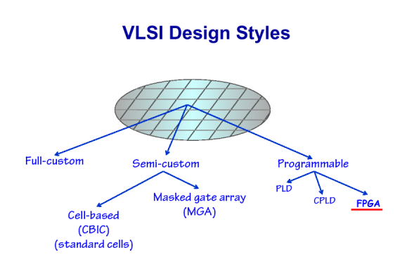
- VLSI Design Styles
lecture 2 - CMOS Circuit Overview
- Transistor Types
- Bipolar transistors
- npn or pnp silicon structure
- Small current into very thin base layer controls large currents between emitter and collector
- Base currents limit integration density
- Metal Oxide Semiconductor Field Effect Transistors
- nMOS and pMOS MOSFETS
- Voltage applied to insulated gate controls current between source and drain
- Low power allows very high integration
- MOS Integrated Circuits
- 1970’s processes usually had only nMOS transistors
- Inexpensive, but consume power while idle
- 1980s-present: CMOS processes for low idle power
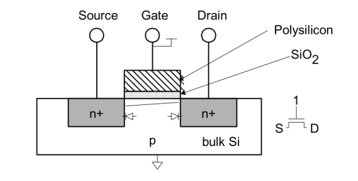
- nMOS Transistor&Operation
Four terminals: gate, source, drain, body
Gate – oxide – body stack looks like a capacitor
- Gate and body are conductors
- SiO2 (oxide) is a very good insulator
- Called metal – oxide – semiconductor (MOS) capacitor
- Even though gate may not be made of metal
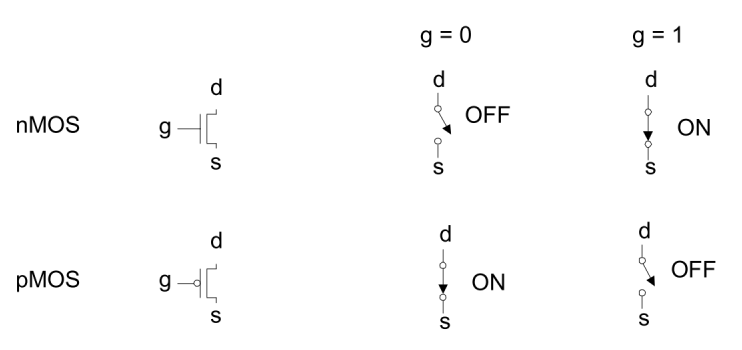
nMOS Operation
- Body is commonly tied to ground (0 V)
- When the gate is at a low voltage:
- P-type body is at low voltage
- Source-body and drain-body diodes are OFF
- No current flows, transistor is OFF
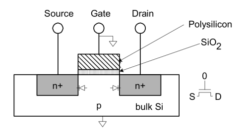
- When the gate is at a high voltage:
- Positive charge on gate of MOS capacitor
- Negative charge attracted to body
- Inverts a channel under gate to n-type
- Now current can flow through n-type silicon fromvsource through channel to drain, transistor is ON
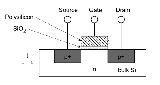
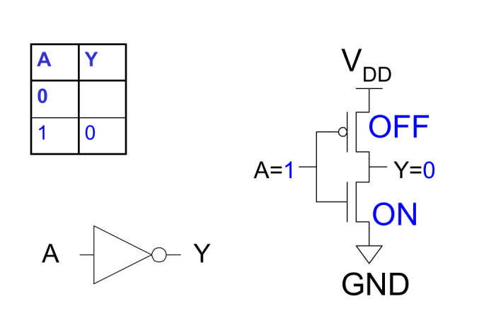
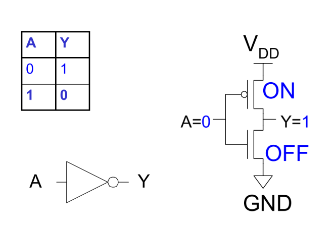
- pMOS Transistor
- Similar, but doping and voltages reversed
- Body tied to high voltage (VDD)
- Gate low: transistor ON
- Gate high: transistor OFF
- Bubble indicates inverted behavior
- Transistors as Switches
We can view MOS transistors as electrically
controlled switches.
Voltage at gate controls path from source to drain.
- CMOS Inverter
- CMOS NAND Gate
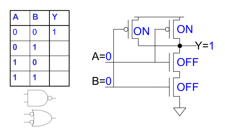
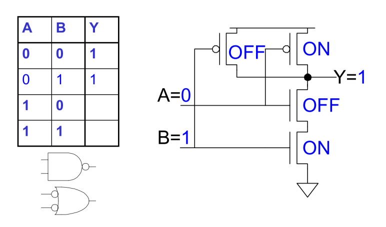
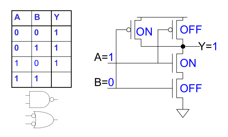
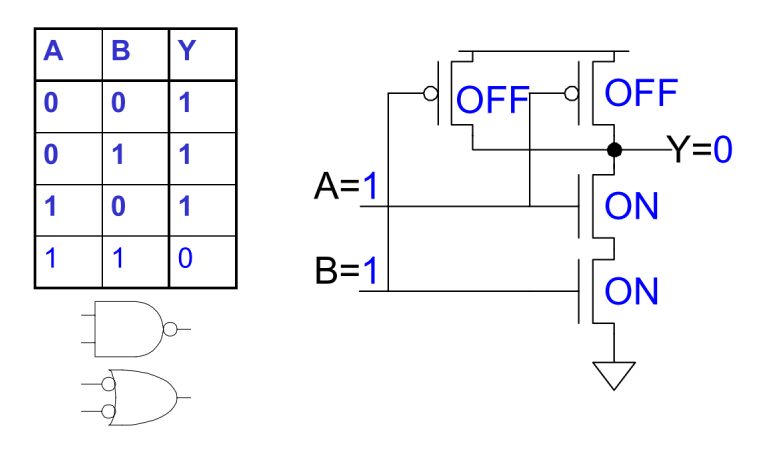
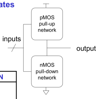
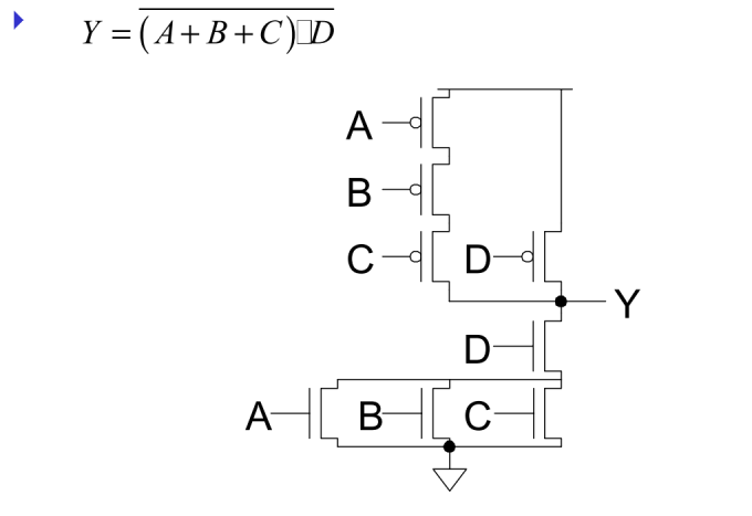
- Complementary CMOS
Complementary CMOS logic gates
- nMOS pull-down network
- pMOS pull-up network
- a.k.a. static CMOS
Rule of Conduction Complements
- Pull-up network is complement of pull-down
- Parallel -> series, series -> parallel
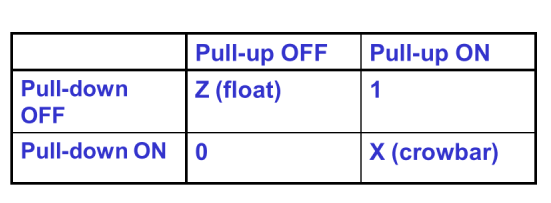
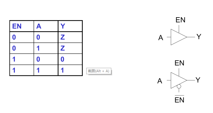
- Tristates
Tristate buffer produces Z when not enabled
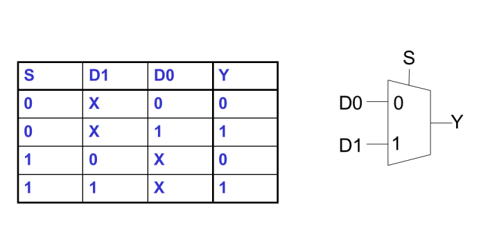
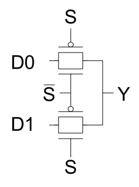
- Multiplexers
2:1 multiplexer chooses between two inputs
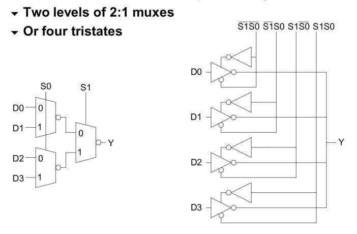
- 4:1 Multiplexer
4:1 mux chooses one of 4 inputs using two selects
- Two levels of 2:1 muxes
- Or four tristates
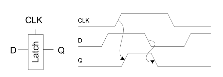
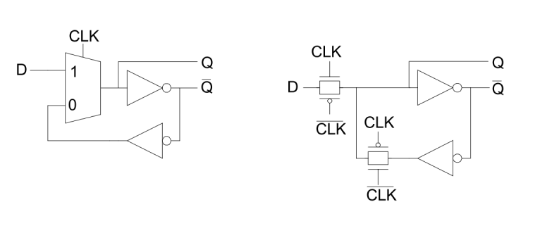
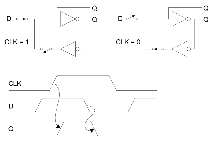
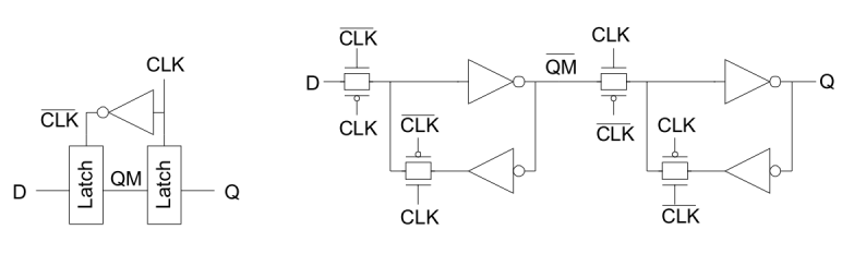
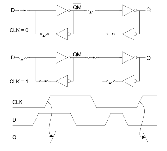
- D Latch
When CLK = 1, latch is transparent
When CLK = 0, the latch is opaque
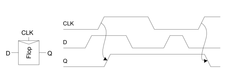
- D Flip-flop
When CLK rises, D is copied to Q
At all other times, Q holds its value
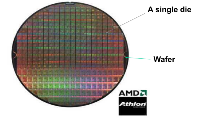
Lecture 3 - Fabrication and Layout
- Wafer Processing
- Czochralski method
- Melt pure polycrystalline silicon in a pot (1400C)
- A seed crystal is dipped to determine the crystal orientation
- Single-crystal ingot is made as polycrystalline silicon is slowly pulled out and freezes
- Silicon ingots have a diameter of 8-12 inches
- Ingots are carefully cut into thin disks (wafers)
- A wafer is typically 200-500um thick
- IC fabrication Process
- Consists of a sequence of processing steps:
Various conducting, semi-conducting and insulating material layers are fabricated to form appropriate 3d device structures
Major processing steps are:
- Lithography
- Oxidation
- Layer deposition
- Etching
- Diffusion
- Implantation
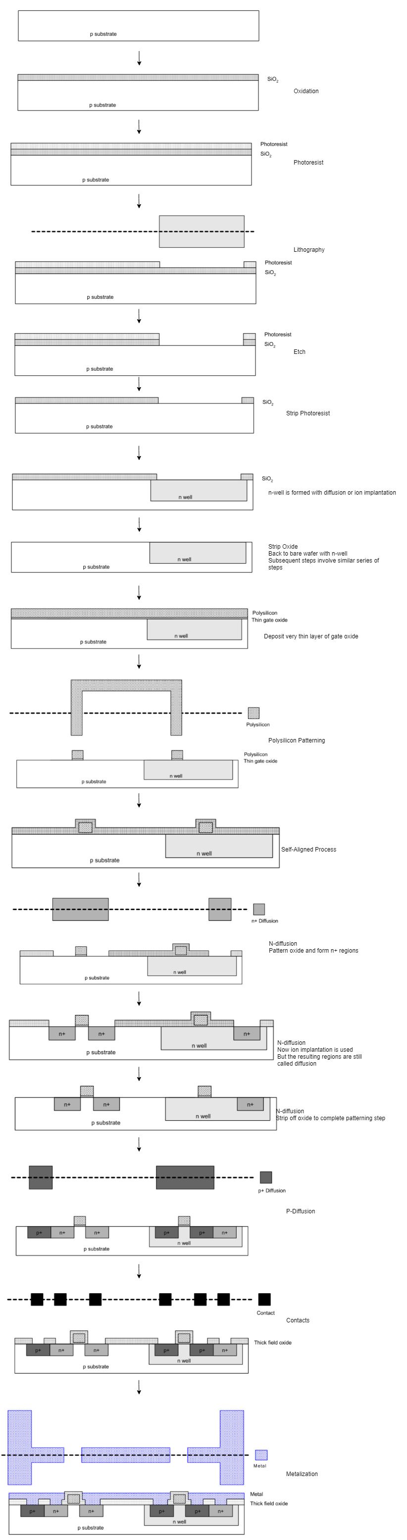
Inverter Cross-section
- Typically use p-type substrate for nMOS transistors
- Require n-well for body of pMOS transistors
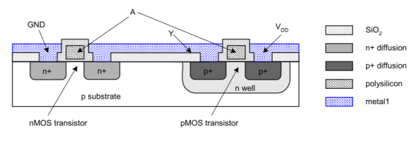
- Well and Substrate Taps
- Substrate must be tied to GND and n-well to VDD
- Metal to lightly-doped semiconductor forms poor connection called Shottky Diode
- Use heavily doped well and substrate contacts / taps
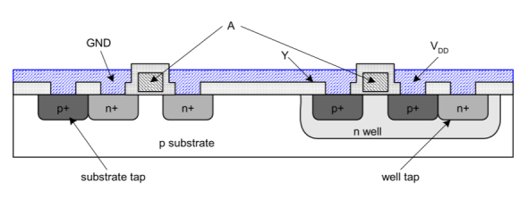
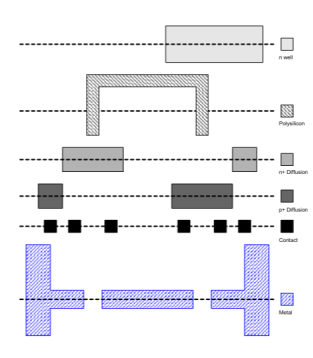
- Inverter Mask Set
- Transistors and wires are defined by masks
- Cross-section taken along dashed line
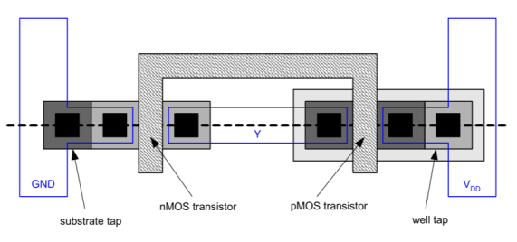
Detailed Mask Views
Six masks:
n-well
Polysilicon
n+ diffusion
p+ diffusion
Contact
Metal
- Fabrication Steps
- Start with blank wafer
- Build inverter from bottom up
- First step will be to form the n-well
- Cover wafer with protective layer of SiO2 (oxide)
- Remove layer where n-well should be built
- Implant or diffuse n dopants into exposed wafer
- Strip off SiO2
- Layout
- Chips are specified with set of masks
- Minimum dimensions of masks determine transistor size (and hence speed, cost, and power)
- Feature size f= distance between source and drain Set by minimum width of polysilicon
- Feature size improves 30% every 3 years or so Express rules in terms of λ = f/2
E.g. λ = 0.3 μm in 0.6 μm process
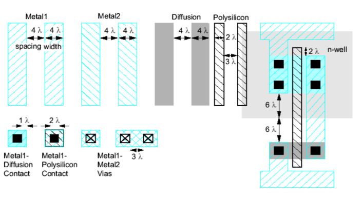
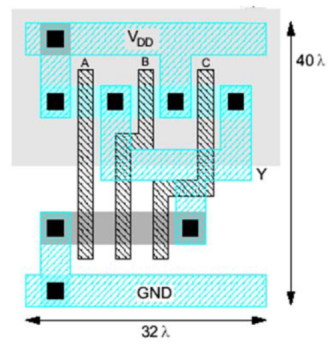
- Inverter Layout
- Transistor dimensions specified as Width / Length
- Minimum size is 4λ / 2λ, sometimes called 1 unit
- In f= 0.6 μm process, this is 1.2 μm wide, 0.6 μm long
- Gate Layout
- Layout design can be very time consuming
Design gates to fit together nicely
Build a library of standard cells - Standard cell design methodology
VDD and GND should abut (standard height)
Adjacent gates should satisfy design rules
nMOS at bottom and pMOS at top
All gates include well and substrate contacts
- Layout design can be very time consuming
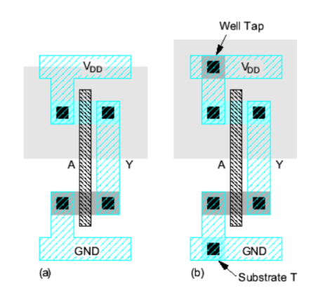
- Example: Inverter
2. AUTOMATIC DIGITAL MODELING FOR ANALOG BLOCKS IN MIXED-SIGNAL VERIFICATION小记
the Institute of Microelectronics, Tsinghua University, Beijing, China
1. INTRODUCTION
混合信号模拟速度限制了芯片的验证速度,从而限制了整个芯片生产的速度。如何提高混合信号的仿真速度是我们需要解决的问题。
纯事件驱动的模拟器过程克服了模拟解算器固有的缓慢性所带来的限制,是实现快速策略的最佳工具。在目前的研究中,混合信号电路到数字电路的转换主要是等效电路法。根据对具体电路的分析,手动生成相应的数字电路。[1] [2]
动态模态分解(DMD)[3] [4] [5]是一种用于流场动力学重建或预测的数据驱动模态分析方法。DMD方法使自动建模成为可能。本文提出了一种基于DMD的自动数字建模算法,该算法可以将SPICE语言中的实际混合信号电路转换为Verilog中的纯数字电路。以SARADC电路为例,验证了该建模算法的可行性。
2. MODELING ALGORITHM
1) 用HSPICE模拟器模拟晶体管级电路;2) 使用DMD方法从原始数据集中提取特征(步骤1);3) 根据步骤2的数据集得到机器学习模型;4) 转换为HDL(数字电路)中的行为级电路;5) 子模块集成和测试台。
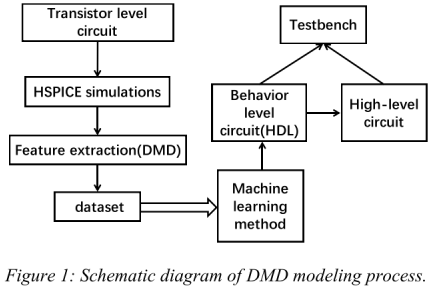
数据采集
对于数字电路,我们通过调整每个信号的周期关系来实现完整的数据输入。我们设置每个输入信号的周期:T,2T,22T,…,2N-1T,然后生成HSPICE电路网表并模拟该网表。通过对所有N个信号进行迭代,得到原始数据集。对于模拟电路,我们很难通过一定的规则生成完整的数据。我们为特定的电路提供特定的输入,或者从整个电路系统中提取仿真结果。
DMD建模
获得训练数据集后,下一步是根据数据集建立和训练模型。建立的模型可以在面对新情况时给出相应的判断。因此,本研究采用DMD方法和机器学习方法对电路输入输出关系进行建模。具体建模实施流程如下:
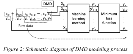
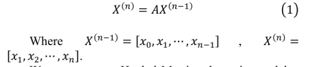
a) 特征提取:在DMD体系结构[3]中,我们可以得到动态系统的方程,如下所示:
我们通过时间延迟嵌入[5]构建Hankel-Matrix矩阵:
然后,我们构造了两个 Hankel-Matrix H1 和 H2,𝐻2 是时移的。 我们将 (1) 转换如下:

参考DMD中Hankel-matrix的构建,我们构建我们的特征空间:
我们假设电路系统的电流输出与当前输入和过去k时刻的输入输出有关,系统对应的输出如下:
b) 建模
对于非线性系统,需要通过先验知识的一定映射,构造出一组足够丰富的可观测量,如核方法和多项式方法[6] [7] [8]。 [4] 使用多层感知器和成本函数 LRSS 来避免手动选择映射方法。 我们的大部分电路都是非线性系统,我们使用机器学习来解决问题。
数字电路的输入输出可以用真值表来表示,因此数字电路选用决策树法。 模拟电路的数据一般为简单的线性或非线性,线性模型一般能满足拟合要求。 我们对更复杂的电路使用神经网络和其他更复杂的方法。
Verilog/Verilog-AM模型
然后我们的 DMD 模型可以转换为 Verilog/ Verilog-AMS 语言。 Verilog/Verilog-AMS 模块可以在顶层模块或测试台中实例化。
Sub-Module Integration
一个复杂的混合信号系统可以拆分为多个子模块,我们为每个子模块建立了 Verilog 模型。 我们可以通过积分得到更高层次的电路,快速验证复杂电路的正确性。
3. APPLICATION TO SARADC CIRCUIT
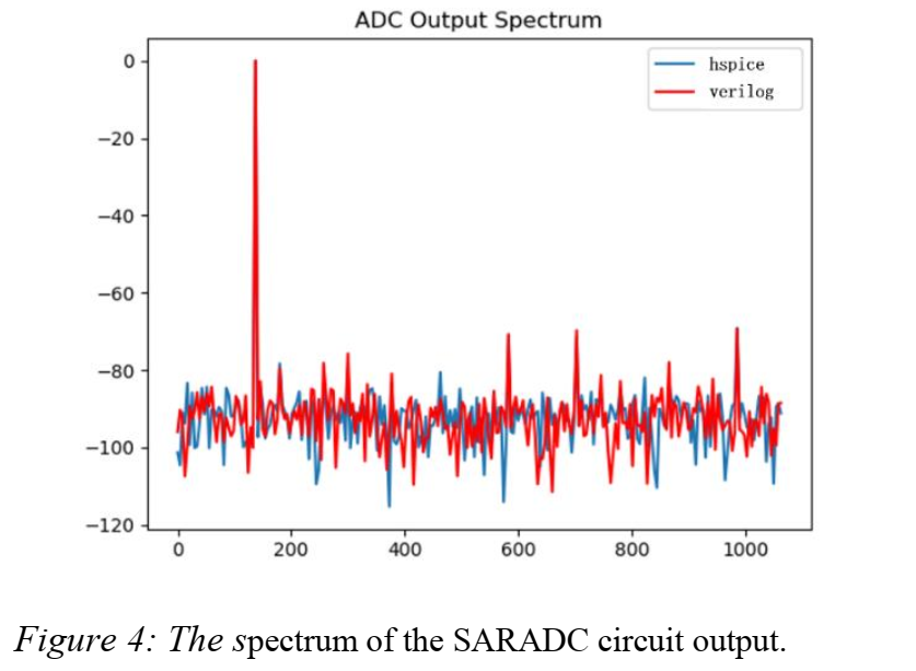
首先,我们将 SARADC 电路建模为一个整体。 为了简化建模,我们将 12 位数字输出信号转换为十进制数。 建模结果如图 3 所示。
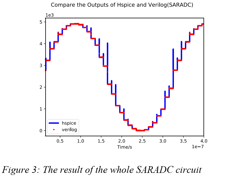
对于 SARADC 电路,我们关注其信噪失真比 (SNDR) 和输出频谱。 所以我们在这两个方面比较了HSPICE仿真和Verilog仿真。
经过计算,HSPICE仿真的SNDR=66.3dB和Verilog仿真的SNDR=65.6dB比较接近。 两次仿真的频谱图如图4所示,可以看出两次仿真的频谱图基本吻合。
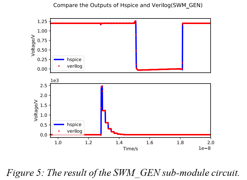
一个电路系统可以分为很多子模块,每个模块都可以通过我们的建模过程进行建模。我们以SWM_GEN模块为例,SC_GEN模块类似于计数器的功能。 我们的建模结果如图 5 所示。
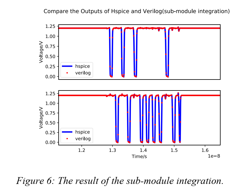
为模拟模块生成的 Verilog 模型可以与任何其他数字模块连接,以进行系统级功能验证。 我们在 SARADC 电路中采用子模块,结果如图 6 所示。我们集成了子模块电路,包括多相时钟生成电路、DAC 电路和比较器电路。
参考文献
[1] Schubert, Martin JW. “An analog-node model for VHDL-based simulation of RF integrated circuits.” IEEE Transactions on Circuits and Systems I: Regular Papers 56.12 (2009): 2717-2727. J. Clerk Maxwell, A Treatise on Electricity and Magnetism, 3rd ed., vol. 2. Oxford: Clarendon, 1892, pp.68–73.
[2] Wegener, Carsten. “Method of modeling analog circuits in verilog for mixed-signal design simulations.” 2013 European Conference on Circuit Theory and Design (ECCTD). IEEE, 2013. K. Elissa, “Title of paper if known,” unpublished.
[3] Kutz, J. Nathan, et al. Dynamic mode decomposition: data-driven modeling of complex systems. Society for Industrial and Applied Mathematics, 2016.
[4] Takeishi, Naoya, Yoshinobu Kawahara, and Takehisa Yairi. “Learning Koopman invariant subspaces for dynamic mode decomposition.” Advances in Neural Information Processing Systems. 2017.
[4] Takeishi, Naoya, Yoshinobu Kawahara, and Takehisa Yairi. “Learning Koopman invariant subspaces for dynamic mode decomposition.” Advances in Neural Information Processing Systems. 2017.
[6] Hofmann, Thomas, Bernhard Schölkopf, and Alexander J. Smola. “Kernel methods in machine learning.” The annals of statistics (2008): 1171-1220
[7] Ham, Jihun, et al. “A kernel view of the dimensionality reduction of manifolds.” Proceedings of the twenty-first international conference on Machine learning. 2004.
[8] Baudat, Gaston, and Fatiha Anouar. “Kernel-based methods and function approximation.” IJCNN’01. International Joint Conference on Neural Networks. Proceedings (Cat. No. 01CH37222). Vol. 2. IEEE, 2001.